cover
THE PUBLISHER
![]()
"SHARE YOUR KNOWLEDGE FOR A BETTER TOMORROW"
Knowledge has power, but it's much more powerful when it is shared
SUBMISSION
JOURNAL METRICS AND INDEXING


Journal of Advanced Research in Applied Sciences and Engineering Technology (ARASET) is licensed under a Creative Commons Attribution-NonCommercial 4.0 International License.
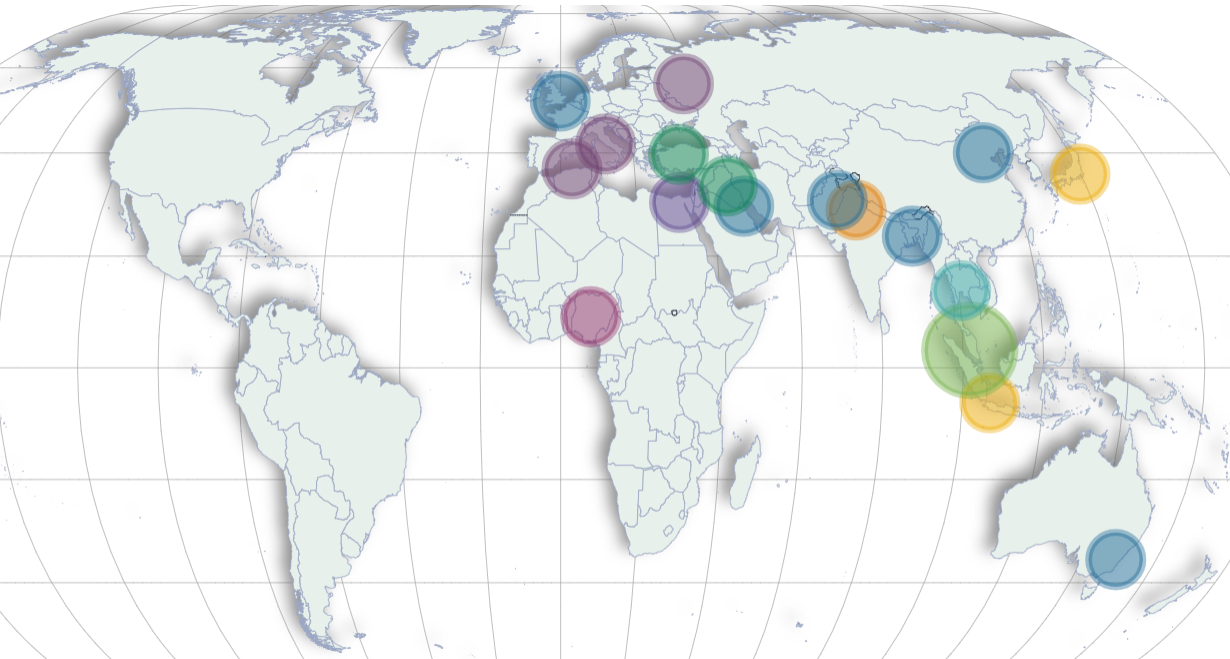
DISTRIBUTION OF AUTHORS